UPDATE: New version of this tutorial is available at the Tutorial 001: Blinking LED x1 page.
 This is very simple tutorial how to make a LED blinking.
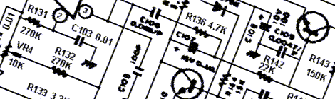
Since the Tinusaur board is a very standard ATtiny breakout board this could be applied to almost any such other board.
The code was tested to work with ATtiny13, ATtiny25, ATtiny45 and ATtiny85 but will probably work other chips too.
We assume that the Tinusaur board is already assembled, successfully; connected through the ISP programmer to the computer; and development environment . It is not the subject of this tutorial how to assemble the board or how to setup development environment.
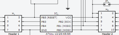
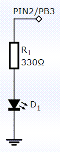
The LED should be connected on pin 2 of the ATtiny – this is PB3 – through a resistor, and to the GND.
The LED, marked as D1, is just a standard light emitting diode.
The resistor, marked as R1, is 270 to 330 ohm.
The most important fragment of the code is this:
	while (1) {
		PORTB |= (1 << LED_PORT);
		_delay_ms(200);
		PORTB &= ~(1 << LED_PORT);
		_delay_ms(400);
	}
What is does is this:
- Start an infinite loop.
- Set the LED wire signal to “1” – that will make it to light.
- Wait a little – 200 milliseconds.
- Clear the LED wire signal to “0” – that will turn it off.
- Wait a little -400 milliseconds.
- Do it again.
Here is the entire source code:
/**
 * The Tinusaur Project
 *
 * Tutorial 001: Blinking LED
 *
 * file: main.c
 * created: 2014-01-04
 *
 **/

#include <avr/io.h>
#include <util/delay.h>

// ====================================
//                ATtiny
//               25/45/85
//              +--------+
//            --+ o  Vcc +------------
//  LED - PB3 --+        +--
//            --+        +--
//  ------------+ GND    +--
//              +--------+
// ====================================

// Define the I/O port to be used for the LED.
// This a number between 0 and 7 that tells which bit to use.
#define LED_PORT PB3

int main(void) {

	// Set the LED port number as output.
	// The DDRB is the data direction for port B.
	// This ...
	//  - shifts the "1" on left to the desired position and ...
	//  - does bitwise "OR" with the value in the port register.
	DDRB |= (1 << LED_PORT);

	// Start infinite loop.
	// (this is how most programs work)
	while (1) {

		// Set the LED bit to "1" - LED will be "on".
		PORTB |= (1 << LED_PORT);

		// Wait a little.
		// The delay function simply does N-number of "empty" loops.
		_delay_ms(200);

		// Set the LED bit to "0" - LED will be "off".
		PORTB &= ~(1 << LED_PORT);

		// Wait a little.
		_delay_ms(400);

		// Do it again ...
	}

	// Return the mandatory for the "main" function value.
	return (0);
}
Copy the code above to your “main.c” file.
The source code could be also found on Bitbucket at this address: https://bitbucket.org/tinusaur/tutorials/src/1f61873ae382/tut001/src/main.c.
The circuit schematics, even though very simple, was drown on 123d.circuits.io and it is available at this address: http://123d.circuits.io/circuits/76781.